retepsnikrep wrote:I'm going to stick with the SV2000 video chip for now for the next Master which will be V2 as we all have some.
At least I will be able to put my SV2000 chip to use.
Moderators: GregsGarage, retepsnikrep
retepsnikrep wrote:I'm going to stick with the SV2000 video chip for now for the next Master which will be V2 as we all have some.
retepsnikrep wrote:Next question. what data available from the Master should I/we log to a PC spreadsheet/data file via the wireless link? I'm assuming here the wireless link is only going to be used when the car is parked up and charging as a safety feature.
Pack Voltage?
Soc?
Charge Current?
Battery Temp?
Charging finished?
Any Alarms?
Fufunka wrote:The following issue/topic has been briefly mentioned perhaps a year ago.
In case of HV system with a dozen ~48VDC modules (full voltage seen
during drive only - broken into modules while charging for safety),
would it be still possible to somehow accommodate this very BMS?
Theoretically, could there be added another layer?
Imagine these modules/subpacks being polled by semi-master pcb, which will then refer up to single top master unit (display out and other functions)? However, these semi-master boards will have to be able to control their local charging units/smart power supplies.
GregsGarage wrote:I will say that is much more voltage than I would feel comfortable working with.
Fufunka wrote:GregsGarage wrote:The issue is not finding a LVC or BMS for it, but rather identifying suitable integrated system, similar to Peter's. Which in this case will have to somehow accomodate the fact that the dc bus is either disconnected during charging and also connected while driving. So there will have to be some sort of aggregate of info polled from these ~dozen subpacks going into the master-board => display etc. under both these modes.
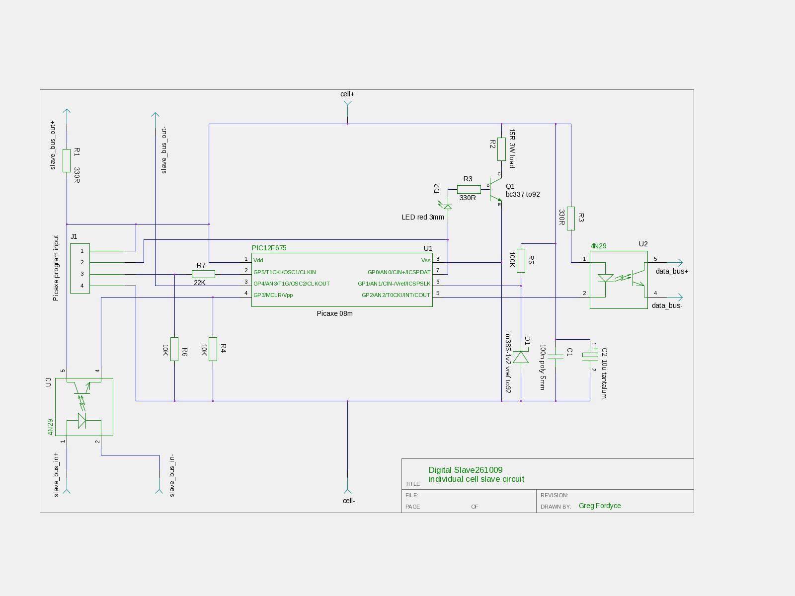
retepsnikrep wrote:Well done Greg. I've looked at your schematic and seems OK.
A few comments.
I like the idea of J2 to supply power I suggest make that a 2 pin sil 0.1" so that you have a simple connector to push on it powered from 3xAA batteries. Or you could make J1 a 4 pin connector (the 4th pin to +ve) and just make up a special programming lead which incorporates the battery supply.
You are proposing a multi connector at the battery box is that correct? My multi cell connector was going to be on the board.
I don't think it will be a problem, R5 on each board should act as a voltage divider to protect individual boards until full connection is made, not sure how D1 in series will affect this though.Imagine the board is ready to go and we plug in a multi cell connector if say the top and bottom pins make contact first how would that effect the board? Or imagine any other combination of pins does it make any difference and is it/could it be detrimental blow the board?
I can add pads if you wanted to connect this way, in my case I will have seperate battery boxes, so it would not be an issueRemember when stacking the multicell slave boards the last + on the bottom board becomes the first negative on the next board up and needs a connector between the two or two wires from that/those terminals at the battery, one for the last + on bottom board and one for first - on next board up.
I will have 1 amp fuses on each cell connection including the first cells negative.Need to try and design it so high current will not try to flow in these wires as well.
I like 16 as well.Finally I think 16 cells is a good number. Because the Master can cope with upto 256 slaves and that divides nicely into it.
As aside I'm learning PicBasic Pro (A compiled much faster system) for my current project, and I may be able to port this knowledge over to make a non picaxe slave which would reduce the cost as we could buy naked chips. (Rick is already tinkering with this) This could be a year away for me though as my current project is pretty tough.
If we wanted to be able to program in situ with this we would need to include the ISCP pins for each slave. I'm not sure about those for the PIC12F683 (Picaxe 08M) or how they would fit in along side the slave schematic. ICSP may not be so much of a necessity as the current picaxe digital slave software I'm using has worked for over a year without any changes or issues. If it works in my Insight I reckon it will work anywhere!!!!
Users browsing this forum: No registered users and 37 guests